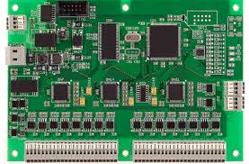
Tutorials: Overview of PCB File Viewers
The PCB File Viewer is a key weapon in the armoury of any electronic designer or engineer. By using this software, users can check and analyze the PCB (Printed Circuit Board) layout details before the physical board is ready to manufacture. The next is critical for design verification which is making sure that the PCB design is compliant with all the requirements, specified, and it should be passed before further into the production.
Maximizing the Advantage of PCB File Viewers
Understanding File Formats
Before using any PCB file viewer properly, you will have to understand what file formats it supports. GerberFiles: The most basic information of the PCB CAD data, The de facto standard file for PCB CAD data, where information about copper layers, solder mask, silk screen is provided, there are many viewers that are compatible with this file format. Being familiar with these formats will make it easier to load and analyze the design files you work with, thus making the work process more streamlined.
Able To Generate Specific Inspections
When it comes to a PCB file viewer, one of the major advantages is the complete visual inspection of the PCB layout. This involves trace width checks, spacing checks, and checks for shorts and opens. By zooming in and out with the pan and scan tools, you can get a close look at particular areas of the circuit, which is essential to catch any problems that might affect the operation of the board or its manufacturability.
Layer Management
In addition, an understanding of how layers can be managed functionally with a PCB file viewer is also needed. Since most PCB designs are made of many layers, being able to hide each layer individually is critical for deeper inspection. This helps you to focus only on certain parts of the circuit, e.g. power planes or signal layers for which you would like to confirm the integrity without the rest of the components getting on the way.
Measurement Tools
Measurement Tools — The measurement tools available in PCB file viewers are also very strong. It allows the dimensions between components, trace lengths, and other critical parameters to be measured right within the viewer using these tools. Precise measurements are necessary to verify the PCB meets design specifications and components align properly throughout the assembly process.
Collaboration and Sharing
PCB file viewers tend to come with options that support team bonding Being able to comment, add notes, or highlight areas in the design will add value in communication between members of the team and can cut down on time that would have been needed to discuss the design during the review process. With this you make sure that anyone on the team could take a look and be on the same page when making design changes.
Automation Features
Automation for ERC and DRC in advanced viewersMost high leveled PCB file viewers include automation functionality for ERC and DRC. Automated tests are quick to conduct and are capable of catching common PCB design mistakes like trace-to-trace clearance, via size, etc. Designers can utilize these tools to make sure that their designs meet industry guidelines, minimizing the potential for expensive post-production changes.
Best Practices with PCB File Viewers
For anyone associated with PCB design, knowing how to use a PCB file viewer can make your life easier…In Conclusion… Designers can improve the quality and speed of design through an understanding of its characteristics and capabilities making sure that each design is more stable and manufacturable that ever reaches the production floor. Not only does this proactive behavior save time and money, but it fosters innovation in PCB design and production.